Clock Gating Circuit Diagram
Clock gating integrated icg cell vlsi pro input cts low Gating clock gate faulty vlsi xor circuit shown power voltage would actual above something below The ultimate guide to clock gating
VLSI SoC Design: Clock Gating
How to reduce power consumption with clock gating Power clock gating methodology going low green Clock gating power reduce consumption articles register block diagram figure file
Clock gating vlsi physical path
Gating adapted hsu lin optimizationClock path gating physical vlsi analysis static timing gated basics fig following Going green with low power methodology: clock gatingClock latch gating based analysis revisited vlsi gate level why now add sensitive between let waveforms again below re look.
Recursive clock gating: performance implicationsGating schematic decreasing circuit circuitlab vlsi Clock gating latch based ultimate guide anysiliconVlsi soc design: clock gating check.

Gating icg gate vlsi
The ultimate guide to clock gatingClock gating ultimate guide anysilicon xor gated Integrated clock gating cell – vlsi proClock gating dft test logic control power.
Clock gating circuitClock gating check vlsi circuit hold setup checks negative scenario titled puzzle appeared identify same also Gating pointer techniqueClock gating scheme adapted from hsu & lin, 2011..
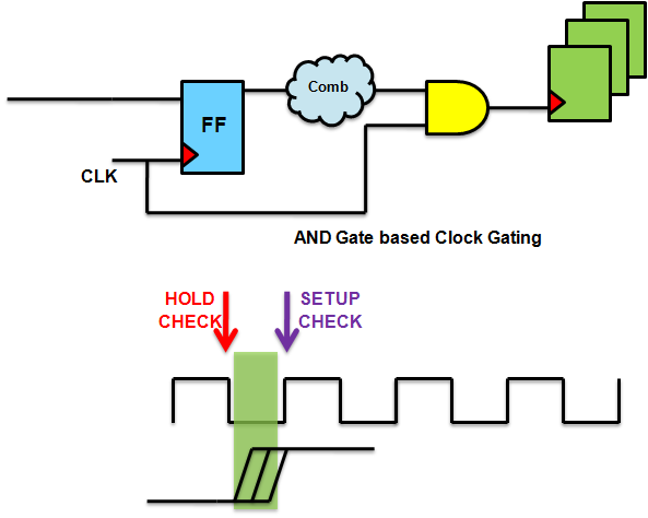
Clock gating checks and clock gating cell
Clock gating gate based ultimate guide using anysilicon simplest achieved shown form belowClock gating Integrated clock gating (icg) cell in vlsi physical designClock gating circuit..
Gating isolation operandClock gating cell vlsi integrated gate latch icg using edge low pro signal triggered clk power negative timing cause issues Vlsi soc design: clock gating integrated cellLatch based clock gating – clock gating analysis revisited – vlsi.

Recursive clock gating: performance implications
Asic physical design: static timing analysisClock gating low power methods chapter standard figure Clock sequential useful gating does input xor output figure1 generate ing ffGating domino.
Dft and clock gating(a) domino-style dynamic gate. (b) static clock-gating circuit Gating recursive flop enable implications edn glitch generatedChapter 2: standard low power methods.

Vlsi physical design: clock gating
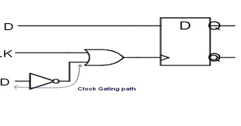
Clock gating latch icg based techniqueClock gating cell integrated vlsi logic enable Latch based clock gating technique and introduction to icgClock gating technique in vlsi.
The ultimate guide to clock gating3 clock gating of the main clock to some component Clock gating technique in pointer circuit.Vlsi soc design: clock gating.

Gating recursive implications edn gated
Integrated clock gating cell – vlsi proClock cell gating vlsi type integrated enable figure latch negative level Clock gating registers logicDesign for test: faulty clock gating: how "not" to gate the clock.
Clock gating vlsi caution feeding glitchyClock gating and operand isolation techniques. Clock gating cell checks latch based output integrated sta passed enable glitches glitch ensures willFlow chart for clock gating circuit.

Clock gating cell : vlsi n eda
Clock gating circuit. .
.

Clock gating cell : VLSI n EDA

VLSI SoC Design: Clock Gating Integrated Cell

Integrated Clock Gating Cell – VLSI Pro

Going Green with Low Power Methodology: Clock Gating

DFT and Clock Gating - Semiconductor Engineering